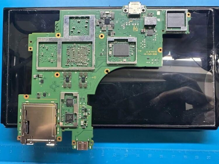
A Redditor who goes by the handle MHN1994 recently posted several images of what is believed to be the PCB of the Nintendo Switch 2, in all its barenaked glory. If this is indeed the circuit board of the Switch 2, it is by far the most detailed shot of the hardware, to date.
One of the screenshots also has a close-up of the NVIDIA SoC that serves as the heart of the gaming handheld, but the person posting it has blurred out the designation on the die. Recent rumours suggest that NVIDIA is providing Nintendo with a Tegra T239 SoC, which features up to 1,536 CUDA cores.
There are several other details to be gleaned from the pictures. It appears that the Switch 2 is also poised to use SK Hynix LPDDR5X RAM which, if earlier rumours are to be believed, is set at 12GB. You can also see the game card slot and what appears to be the USB-C port at one end of the PCB, which we’re guessing is the top of the console.
Next to Sony’s PlayStation 5 Pro (PS5 Pro), the Switch 2 has been Nintendo’s worst kept secret of 2024, even if the game company has made sure that its lips have been absolutely airtight. Just last month, multiple third party accessory makers including dbrand broke cover with the console, showing it off with their casings.


The Switch 2 is expected to launch sometime within the first quarter of this year, although when exactly is still a mystery.
Follow us on Instagram, Facebook, Twitter or Telegram for more updates and breaking news.


