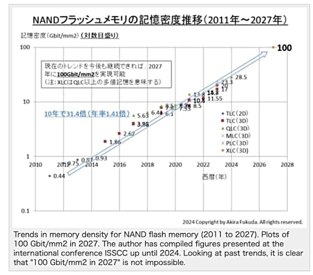
Kioxia, the Japanese memory maker, seems to be on the road towards increasing the density of NAND flash memory cell layers by as much as 1,000 layers on a single die, or 100 Gbit/mm2.
3D NAND layers have rapidly increased over the past decade, going from 24 layers back in 2014 to 238 layers today, and that is going to continue increasing. In the eyes of Kioxia, the memory maker believes it can hit the 1,000-layer mark by 2027.

As per a report by the Japanese outlet, PC Watch: “Kioxia predicts that memory density will reach 100 Gbit/mm2, and the number of word line layers (number of memory cell layers) will reach 1,000. Based on the announcement from ISSCC, an international conference on cutting-edge semiconductor circuit technology, both memory density and number of layers will be more than three times higher than in 2023-2024.”
As ambitious as the plan is, Kioxia is aware that scaling to a four-digit layer count will not be easy. As pointed out by Blocks & Files, there’s more to it than just adding layers to the chip. “Increasing density in a 3D NAND die isn’t just a case of stacking more layers on the die, because an edge of each layer needs exposing for wordline electrical connectivity. This gives the die a staircase-like profile and, as the layer count increases, so too does the area of the die needed for the staircase.”

Whether or not the Japanese memory maker will be able to achieve this dream is still up in the air. As it stands, the company and its manufacturing partner, WD, will be looking forward to bringing their BiCS 8 technology with 218 layers into mass production, followed by plans to bring about its BiCS 9 and 10 technology, both of which should have 3D NAND chips running with over 400 layers.
(Source: PC Watch, Blocks & Files, Techspot)
Follow us on Instagram, Facebook, Twitter or Telegram for more updates and breaking news.


