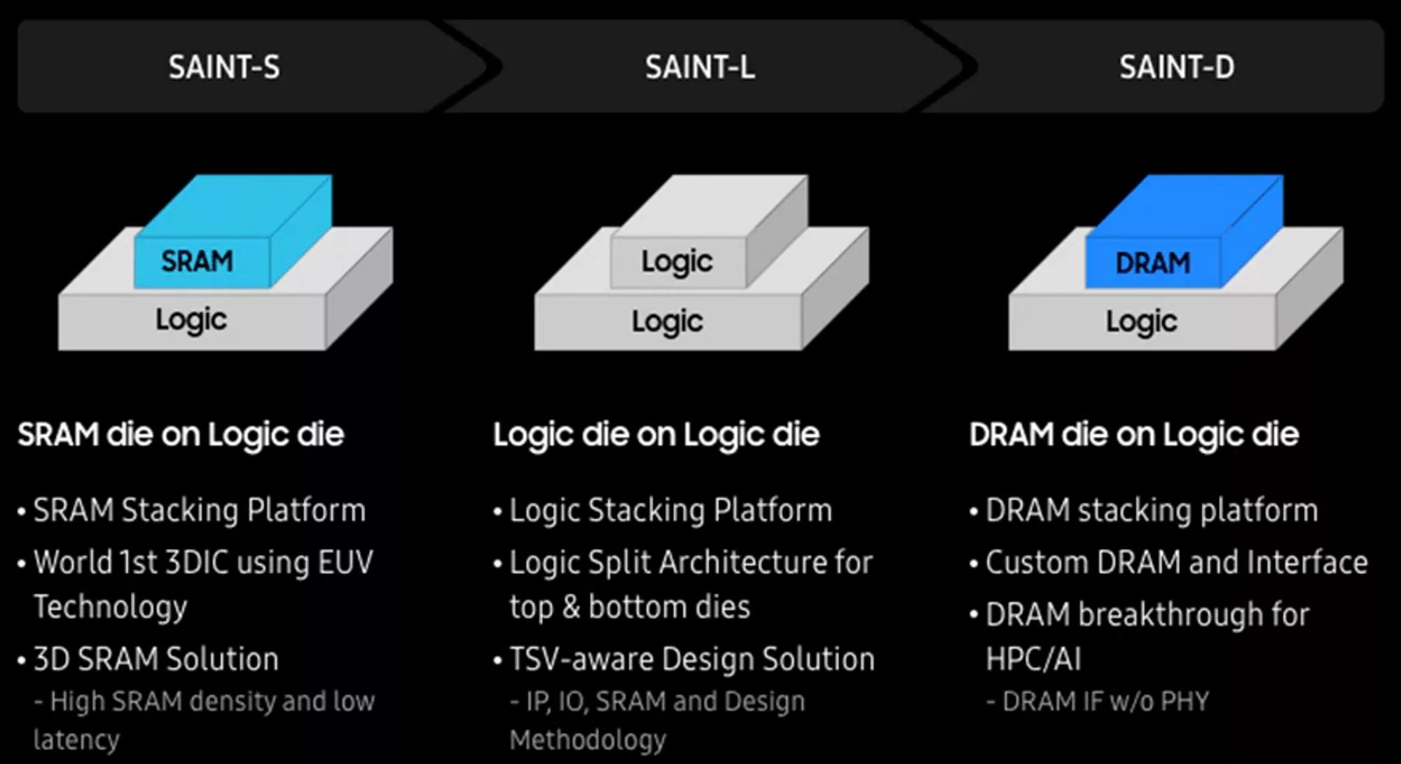
Samsung revealed its latest and most advanced chip packaging technology during its annual Samsung Foundry Forum 2024 in the US earlier this month. According to the Korean Economic Daily (KED), the new technology, dubbed HBM4, will be the first time the Korean electronics giant unveiled 3D stacked technology.
The event marked the first time that its 3D stacked packaging technology, also known as SAINT-D, came weeks after Jensen Huan, CEO of NVIDIA, unveiled his company’s next-generation Rubin architecture, which is only expected to hit the market in 2026.

The 3D stacked packaging technology is an important next step for Samsung, more so for the HBM memory standard. At current, HBM memory are primarily packaged using the 2.5D packaging technology.
With 2.5D, HBM chips are horizontally connected with a GPU on the silicon interposer. With 3D stacked technology, a silicon interposer isn’t needed and instead, a thin substrate is placed between the chips, allowing components to communicate and work together faster.

The application of 3D stacked HBM chips isn’t just limited to GPUs too. With this, Samsung could also begin stacking the chips on CPUs as well, enabling the same improvement in performance, in theory. That being said, implementing the new packaging also means higher manufacturing cost, which is why Samsung is reportedly interested in offering it as a “turnkey” service. In other words and as it is always the case, it’s doubtful that the technology see the light of day in the consumer space.
(Source: KED, Techspot, Hot Hardware)
Follow us on Instagram, Facebook, Twitter or Telegram for more updates and breaking news.


