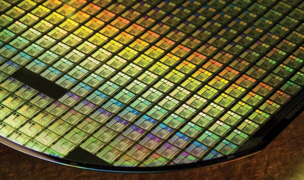
TSMC recently announced that its performance-optimised N3P process node, will enter mass production in the second half of this year. The new and improved process follows closely after the fab’s successful rollout of its current-gen, 3nm N3E process, and is an optical shrink that it claims will provide better efficiency and transistor density.
According to AnandTech, TSMC says that it is already seeing “great” yields with its second-generation 3nm process node. “N3E started volume production in the fourth quarter of last year, as planned,” a TSMC executive said at the event. “We have seen great yield performance on customers’ products, so they did go to market as planned.”
As N3P is an optical shrink of N3E, the new process node should be compatible with its predecessor in terms of IP blocks, process ruls, and design methodologies, to say the least. “We have also successfully delivered N3P technology,” the TSMC executive said. “It has passed qualification and yield performance is close to N3E. [The process technology] has also received product customer tape outs and will start on production in the second half of this year. Because of [PPA advantages] of N3P, we expect the majority of tape outs on N3 to go to N3P.”


