As the world preps itself for the advent of 3nm die lithography, TSMC is working hard on making the necessary preparations to bring its 2nm process into mass production. To that end, the Taiwanese foundry will be turning to what is clearly the inevitable step in doing so: an AI-assisted process.
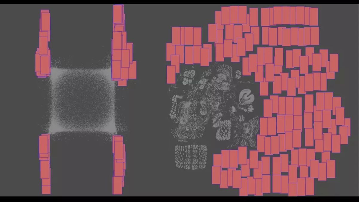
More to the point, TSMC’s 2nm manufacturing process will be using an AI-enhanced method known as AutoDMP and interestingly enough, the process itself will be powered by NVIDIA’s DGX H100 GPU, which the latter spoke at length at its keynote at Computex 2023, that took place at the end of the month. As to why the company is resorting to the aid of AI, the answer is quite obvious – compared to manual labour, using the AI process would expedite the manufacturing process by approximately 30 times and, as a result, improve energy efficiency and decrease carbon emissions.

If it also wasn’t obvious, TSMC is currently in a race to be the first to introduce 2nm to the market, and more specifically by 2025. If the company manages to meet its allotted deadline, the process would effectively be the world’s first 2nm process to be made with gate-all-around (GAA) transistors. This is all new for the manufacturer, so we also wouldn’t be surprised if and when it runs into any difficulties in the process.
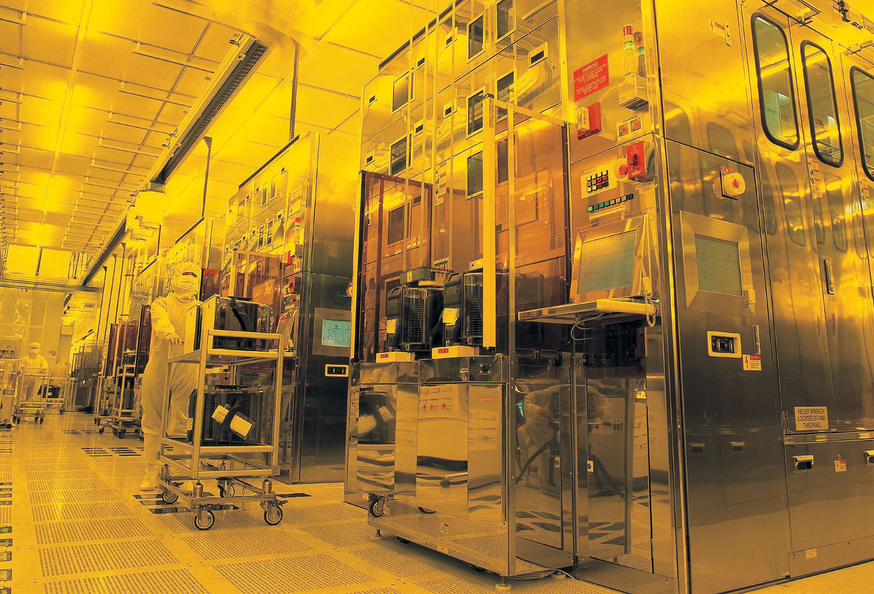
For now, TSMC is aiming for a small-scale production line, with the aim of producing 1000 wafers of the 2nm process this year, according to engineers and support workers from the Zhuke R&D plant in Baoshan, Taiwan, who spoke to the Taiwanese news portal, Economic Daily. Trial productions are expected to conclude by next year and while nothing was confirmed, it is likely that the foundry will expand said Zhuke facility and even open a new plant at Taichung. Beyond that, no further details were mentioned.
(Source: Economic Daily via Tom’s Hardware, Techspot)
Follow us on Instagram, Facebook, Twitter or Telegram for more updates and breaking news.


