The Sony PlayStation 5 has been on the market for nearly a year now and while it is a known fact that the console is being powered by a System-on-Chip (SoC) designed and made by AMD, there aren’t actually a lot of close-ups of the die. Until now.
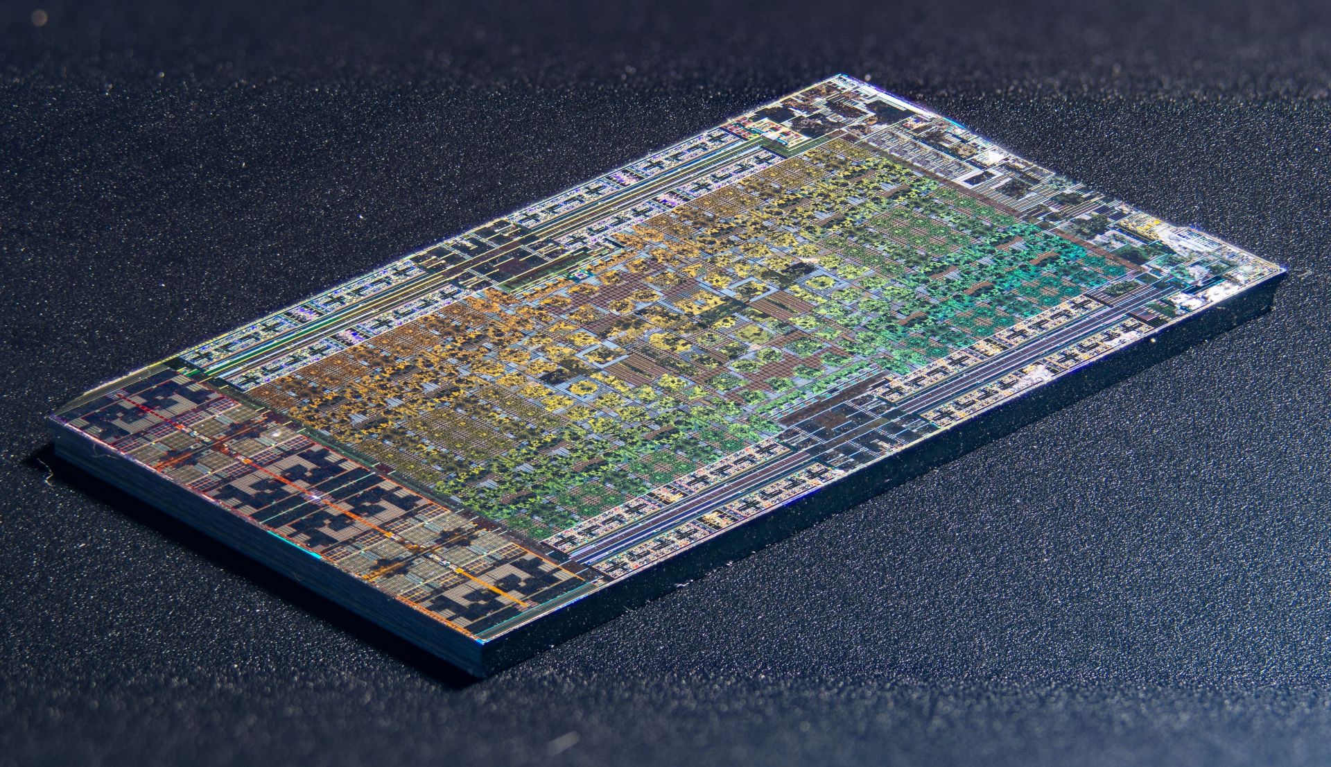
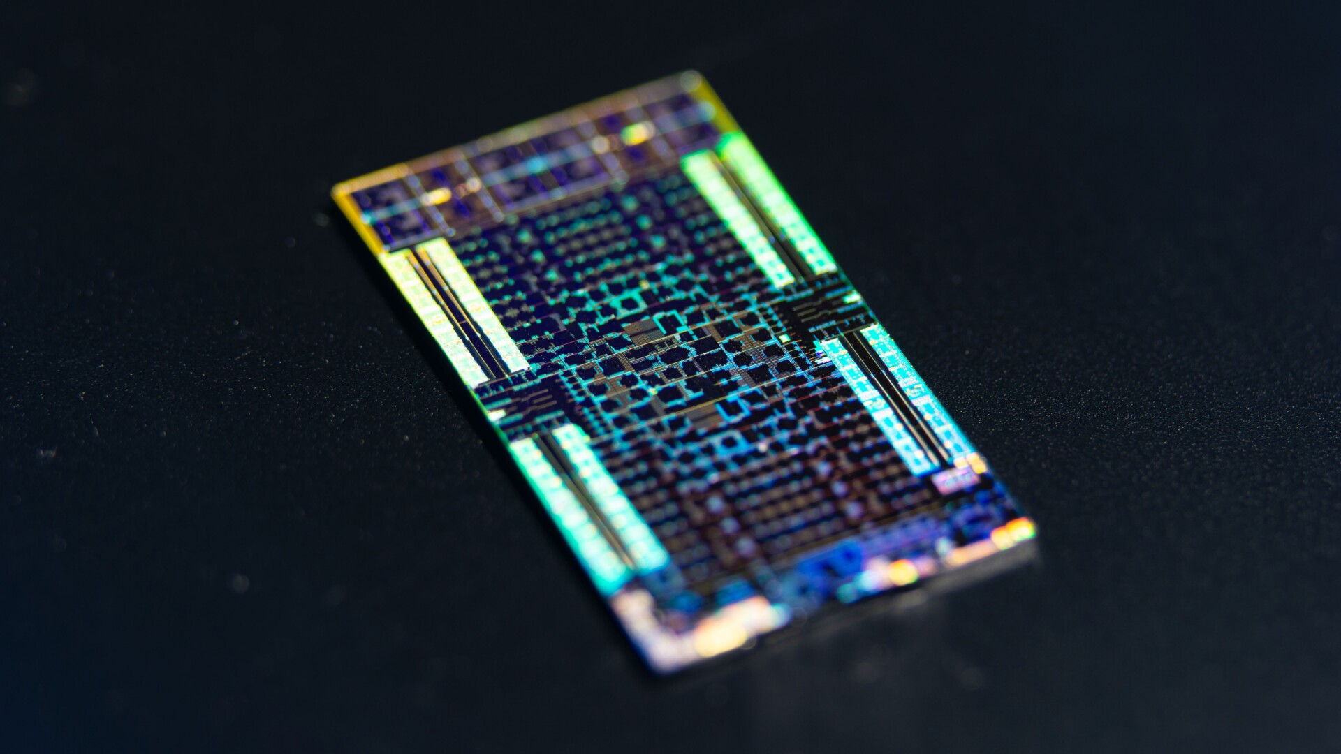
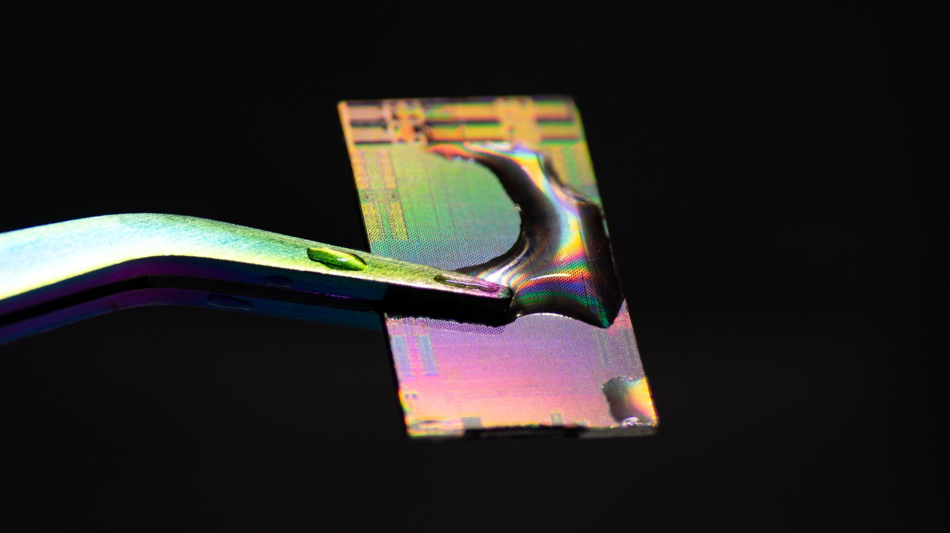
Thanks to the efforts of a hardware enthusiast by the name Fritzchens Fritz, we finally have a close-up shot of the AMD die – codenamed Oberon, by the way – and all the billions of transistors that make it up. Needless to say, Fritz’s close-ups of the component are breathtaking and, for lack of a better word, magnificent and give us a really clear look at its architecture.
In one die shot, you can actually see the GPU core right in the middle, flanked by Zen 2 Cores and the CUs that make up the chip’s GPU engine. In another image, the GDDR6X memory controller and physical layer interface are visible around the edge of the SoC. In the same image, you can also see the L3 Cache.

It is believed that the die Fritz has originated from an AMD 4700S desktop kit. Specifically, it is believed that these chips in these kits are ones that didn’t pass Sony’s and AMD’s quality control and as such, are repurposed as desktop kits.
As a quick recap, the AMD Oberon SoC, is used in both Sony’s PlayStation 5 and Microsoft’s Xbox Series X and S consoles. At its core, the SoC is powered by eight Zen 2 CPU cores running at 3.5GHz, and up to 36 RDNA2 CUs chugging along at 2.23GHz.

If you’re interested, you can check out more close-up images of Fritz’s die, which he has posted on his official Flickr page.
(Source: Fritzchens Fritz via Flickr, Tom’s Hardware, Techspot)
Follow us on Instagram, Facebook, Twitter or Telegram for more updates and breaking news.


