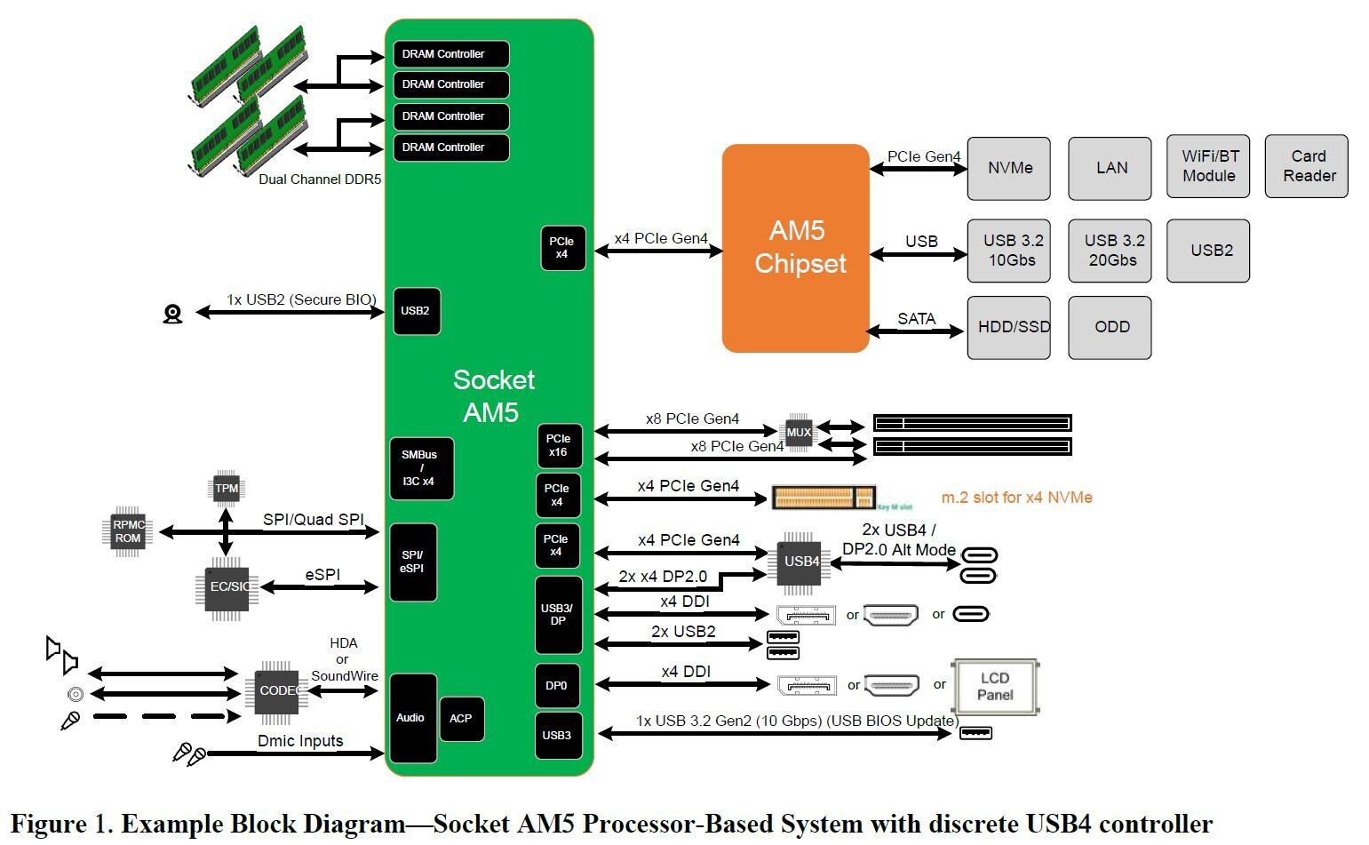
A leaked block diagram, detailing AMD’s Socket AM5, is suggesting that the next-generation platform for Team Red may not be jumping on the bandwagon for PCIe 5.0 interface, which is expected to make its debut later this year with the launch of Intel’s 12th generation Alder Lake-S CPU.
Based on the diagram, AM5, codenamed “Raphael”, will still retain the use of PCIe 4.0, but on the bright side, the chipset will be the first AMD platform to adopt the dual-channel DDR5 memory standard. Further analysis of the diagram also shows that AM5 CPUs will be capable of outputting as many as 28 PCIe 4.0 lanes, 16 of which are expected to be allocated towards discrete graphics, four for CPU-attached M.2 NVMe slots, four lanes for a USB 4 controller, and the remainder to chipset-bus.
One important point to note is while the diagram mentions the adoption of DDR5, it doesn’t specify the memory’s maximum supported speed.

The revelation is also just a little surprising, especially when you consider AMD’s propensity to either be the first adopter and the one spearheading the adoption process of the latest interface, in the same it gradually shifted the balance of power from Intel, first with its Ryzen lineup, followed by its adoption of the current PCIe 4.0 interface.
As for where TPU obtained the diagram? Based on its short report, the tech site apparently obtained the data from confidential Gigabyte documents that were ill-gotten by the RansomExx hacker group. From the looks of it, a fallout occurred between the two parties, leading to the threat actors leaking several gigabytes worth of data via its own site.
(Source: TPU, Videocardz)
Follow us on Instagram, Facebook, Twitter or Telegram for more updates and breaking news.


