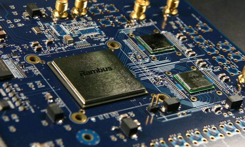
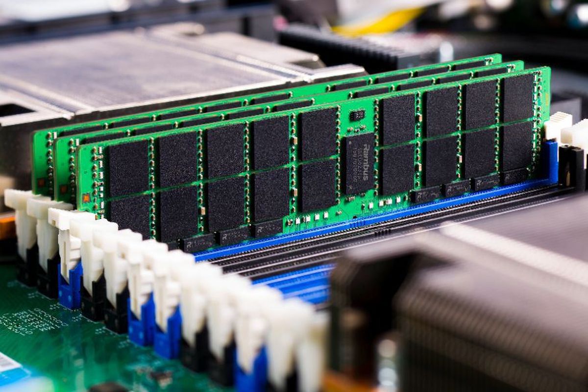
Rambus, a US-based chip and semiconductor maker, recently announced its HBM3-ready memory interface subsystem. The subsystem comprises a fully integrated PHY, as well as a digital controller.
On paper, Rambus says that its new HBM3-ready memory is capable of supporting data rates as high as 8.4Gbps. To put that number into another context, that’s a memory bandwidth of one terabyte per second, which is even greater than the current HBM2E memory on the market.
Rambus says that the creation of HBM3-ready memory was due to the memory bandwidth requirements that are currently being dictated for Artificial Intelligence (AI) and Machine Learning (ML) training machines. In addition to its higher-than-average data rates, Rambus says that its HBM3-ready memory also supports RAS features, includes built-in hardware-level performance activity monitor, and is capable to deliver full bandwidth performance across all data traffic scenarios.

In addition, the memory includes 2.5D package and interposer reference design, and even features a LabStation development environment that provides quick system bring-up, characterisation, and debugging.
If you’ve never heard of Rambus before, you’d be forgiven for a number of reasons. Founded in 1990, the company was the first to invent and develop the 600MHz interface technology and served as the bedrock for many components in the 90s, including the dynamic random access memory (DRAM) component. Moreover, the company shares a patent license with NVIDIA, the latter having access to Rambus’ patent portfolio, such as serial links and memory controllers.
(Source: Rambus // Image: Fortune)
Follow us on Instagram, Facebook, Twitter or Telegram for more updates and breaking news.


