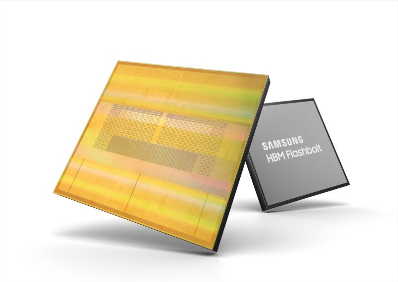
Earlier this week, Samsung launched “Flashbolt”, its newest and fastest memory standard to date. The new memory is based on the brand’s 3rd generation High Bandwidth Memory 2E (HBM2E), is designed for high performance computing (HPC) systems, and seemingly comes in a single 16GB capacity.
The new memory HBM2E standard is obviously a direct successor to Samsung’s last generation Aquabolt HBM2, which also had half the capacity at 8GB. To achieve this high capacity, Samsung says that it had stacked eight layers of 10nm, 16-Gigabit DRAM dies. Vertically and on top of a buffer chip. Further, the new HBM2E package has the dies interconnected through more than 40000 “through silicon via” microbumps.
 On paper, Flashbolt has an average transfer speed of 3.2Gbps and a memory bandwidth of 410GB/s per stack. However, Samsung says that its new HBM2E is capable of attaining faster transfer speeds. Having achieved speeds of up to 4.2Gbps, with a memory bandwidth of 538GB/s per stack.
Volume production of Flashbolt is expected to go into full motion sometime during the first half of this year. Availability has yet to be announced, but for now, Samsung says that it will continue providing its Aquabolt solutions to its clients.
(Source: Samsung)
Follow us on Instagram, Facebook, Twitter or Telegram for more updates and breaking news.


