The folks at iFixit have finally gotten their hands on the iPhone X. The resulting teardown shows a device that packs a huge amount of technology into a single device; with some interesting solutions to get around space limitations; including the dual battery setup we saw before.
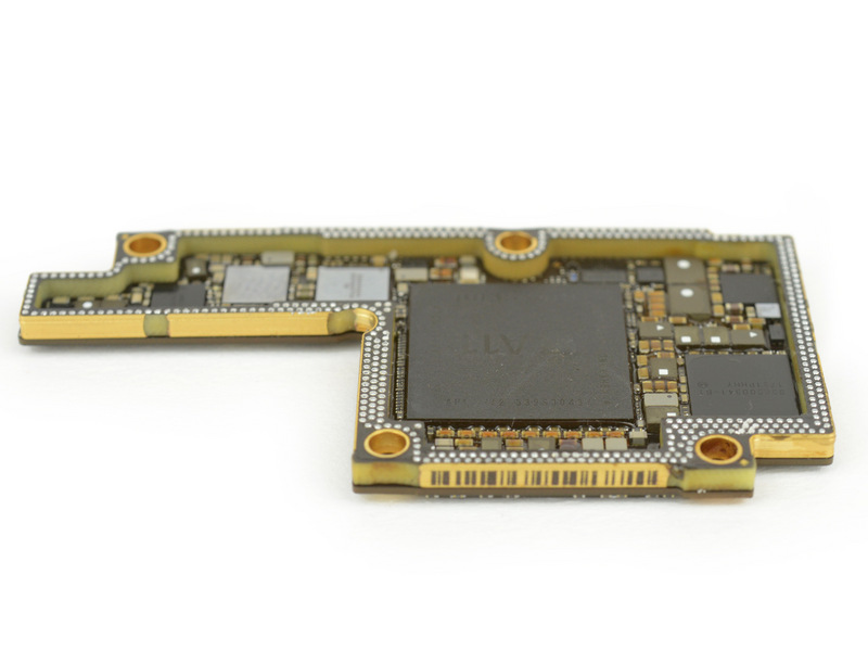
While the battery arrangement was certainly a curiosity, the double layered printed circuit board is a marvel of engineering. Apple’s designers managed to create a PCB sandwich to reduce its footprint, while also increasing the amount of components that could be fitted into the same space.
iFixit estimates that the folded PCB takes up about 30% less space than the one in the iPhone 8; it also managed to create 35% more space for components. The double layer was achieved by adding a spacing layer along the perimeter of the PCB. This also manages to connect the top and bottom layer without the need for cables.
 These space saving solutions appears to have been necessary to make space for the new TrueDepth camera system. Which doesn’t only take up more space in the phone that a regular camera would, but also introduces the first time that Apple has made a front panel that separates without the camera.
Apple’s iPhone X is probably the most advanced phone it has ever created, and should put a stop to all those complaints about the company not innovating. Especially when we take into account just how much work has gone into cramming as much as possible into such a small device. Then again, that probably explains the exorbitant price tag.
[Source: iFixit]
Follow us on Instagram, Facebook, Twitter or Telegram for more updates and breaking news.


