JEDEC Solid State Technology Association – an independent semiconductor trade organisation – has recently announced an update to HBM (High-Bandwidth Memory) technology called: JESD235 or more commonly known as HBM2. Interestingly, there are only a handful of graphics cards that are currently using first generation HBM technology, which is understandable since HBM technology is still quite new.
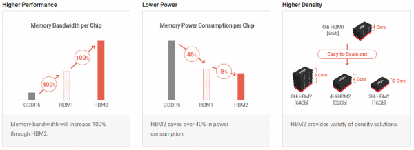
Initially, HBM1 technology came with a maximum bandwidth of 128GB/s with a minimum capacity per layer of 256MB. With HBM2, the maximum bandwidth was increased twofold, making the maximum bandwidth now at 256GB/s along with a minimum capacity per layer of 512MB . In addition to that, JEDEC mentioned that HBM2 will be available either 2-high, 4-high or 8-high TSV (through-silicon via) stacks.

Besides that, JEDEC has also stated that it has included a new pseudo channel architecture to further enhance the bandwidth of the HBM2. That’s not all, HBM2 comes with alert controllers to take necessary actions when the DRAM exceeds maximum operational temperatures. JEDEC HBM Task Group Chairmain, Barry Wenger, says that JEDEC has come up with a perfect solution meet the demands of reducing the footprint as well as significantly increasing the performance of GPUs and CPUs.
Currently, there are yet to be any GPUs released with HBM2. However, according to rumours, Nvidia and AMD may utilise HBM2 for their upcoming GPU designs. Currently, one of the most powerful graphics card in the market, the GTX Titan X, has 12GB of VRAM. With the upcoming release of GPUs by AMD and Nvidia using HBM2, 12GB is not only possible, but could also be increased up to 32GB.
With the introduction of VR gaming and an increase in performance hungry games, HBM2 couldn’t have come at a better time. A full comparison between previous generations of DRAMs against HBM2 can be found here.
(Source: VideoCardz , TechPowerUp)
Follow us on Instagram, Facebook, Twitter or Telegram for more updates and breaking news.


