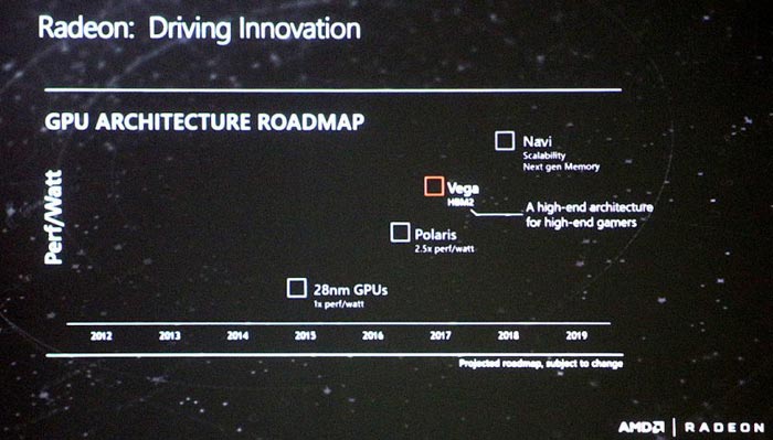
Updates regarding AMD’s next generation GPUs – the Vega 10 and Vega 20 – have been discovered. Key specifications of both the GPUs were obtained through AMD’s own ‘internal’ server roadmap.
The Vega 10 is believed to come with 64 CUs (compute units) along with 24 TFLOPS of FP16 (half precision floating-point) performance. AMD’s Vega 10 GPU is also said to be based on its 14nm GFX9 (internal codename) architecture. One of the highlights to this GPU would have to be its 16GB HBM2 memory that is capable of bandwidth speeds of up to 512GBps. All of this would amount to a TBP (typical board power) of around 225W. Interestingly, AMD is also rumoured to be releasing a dual Vega 10 GPU graphics card in Q2 of 2017.

Next up is the significantly more powerful AMD Vega 20 GPU. Unlike its less powerful sibling, the Vega 20 GPU will be based on a 7nm GFX9 architecture. It’ll be equipped with 32GB of HBM2 memory that should, theoretically, be able to achieve bandwidth speeds of up to 1TBps. In addition, this GPU is also rumoured to have a TBP of 150W. One never before seen feature that is said to be added onto Vega 20-based graphics card(s) would be PCIe 4.0 support, which is rumoured to be arriving sometime next year.
Another GPU that was mentioned by VideoCardz is the Vega 11 GPU. No specific details were given regarding the GPU other than the fact that AMD will most probably be planning to use Vega 11 to replace Polaris 10.

Regardless, if these rumours were to be believed, then it would mean that AMD is currently planning to release several graphics cards next year that would be able to compete with Nvidia’s top of the line mainstream offerings. As always, take these rumours with a pinch of HBM2 salt folks.
(Source: VideoCardz)


