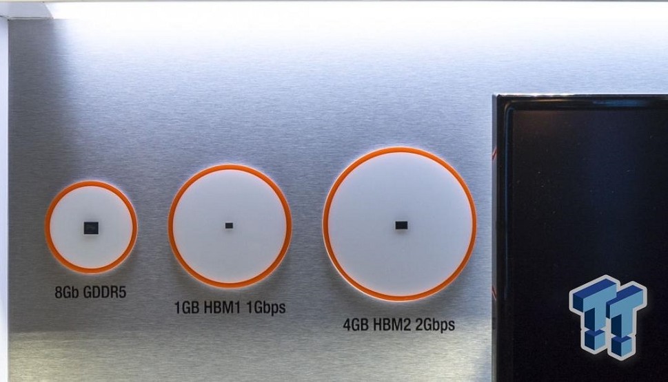
During Nvidia’s GPU Technology Conference, SK Hynix – Nvidia’s semiconductor partner – has shown attendees just how significant the HBM2 memory standard really is in terms of die size. For comparison, SK Hynix has also laid two other memory standards (GDDR5 and HBM1) alongside HBM2.
Despite being the smallest, HBM1 still only contains about half the bandwidth speed that HBM2 can churn out; it also has four times less memory capacity. GDDR5, on the other hand, has the largest die size, but it has more or less the same capacity as HBM1 (8Gb = 1GB).

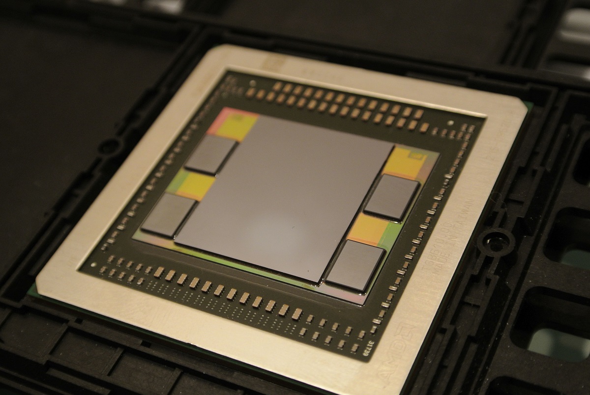
The crème de la crème, HBM2, outmatches both GDDR5 and HBM1 memory standards in terms of bandwidth speeds and capacity, despite being slightly larger compared to HBM1. To put this into perspective, AMD’s R9 Fury X had 4GB of HBM1 memory when it was released. SK Hynix has managed to replicate the performance and capacity of 4-Hi stacks of HBM1 onto a single die called HBM2. Just imagine the possibilities.
When HBM2 is widely available to GPU manufacturers like AMD and Nvidia, one shouldn’t be surprised to see GPUs with, say, more than 16GB of VRAM in the future. Some might argue that more VRAM isn’t really necessary for gaming, but with the imminent arrival of VR games, GPU memory capacity will definitely need a rise.

Unfortunately, it seems that there is little chance for gamers and PC enthusiast to see a consumer-class GPU being released with HBM2 this year. Currently, only Nvidia’s recently announced Tesla P100 is coming with the memory standard, which isn’t meant for average consumers. Hopefully, come next year, HBM2 will be widely implemented.
(Source: TweakTown)
Follow us on Instagram, Facebook, Twitter or Telegram for more updates and breaking news.


