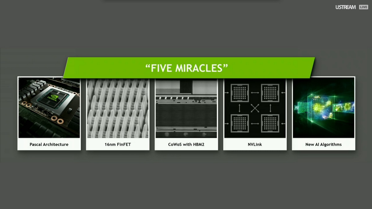
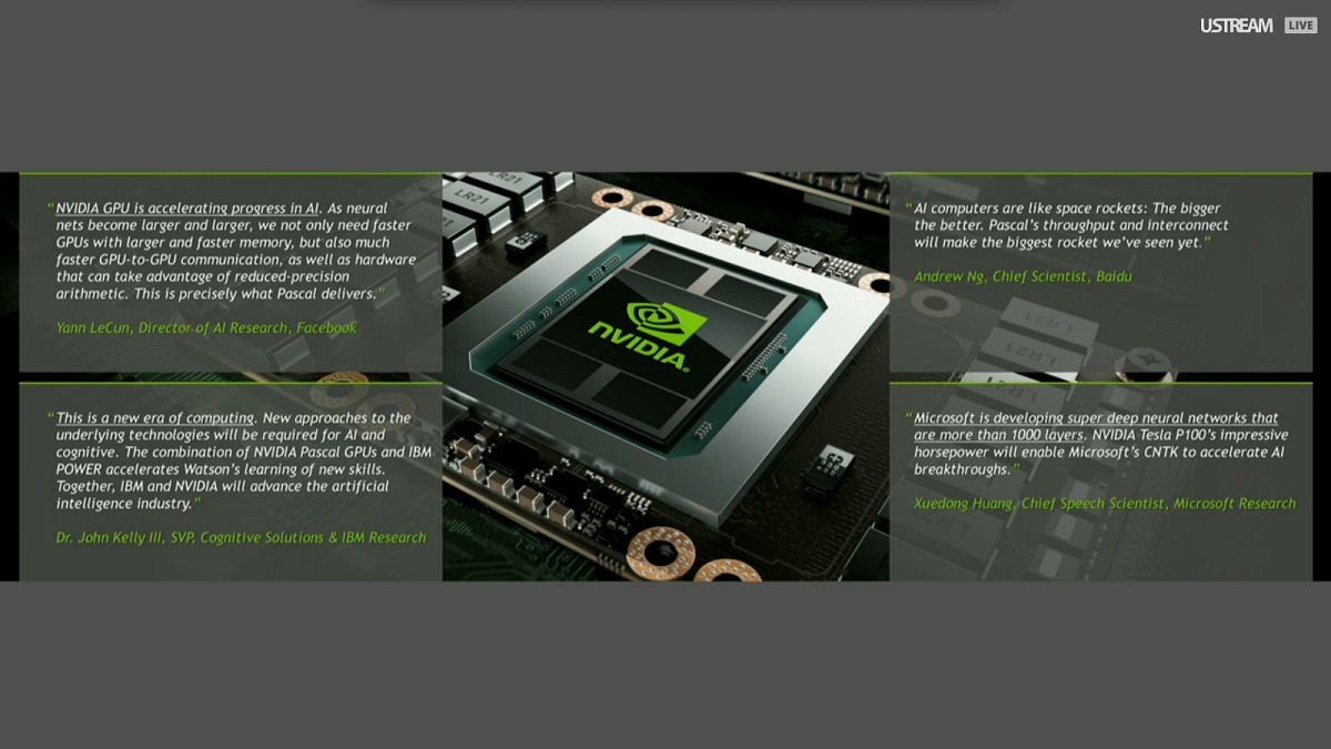
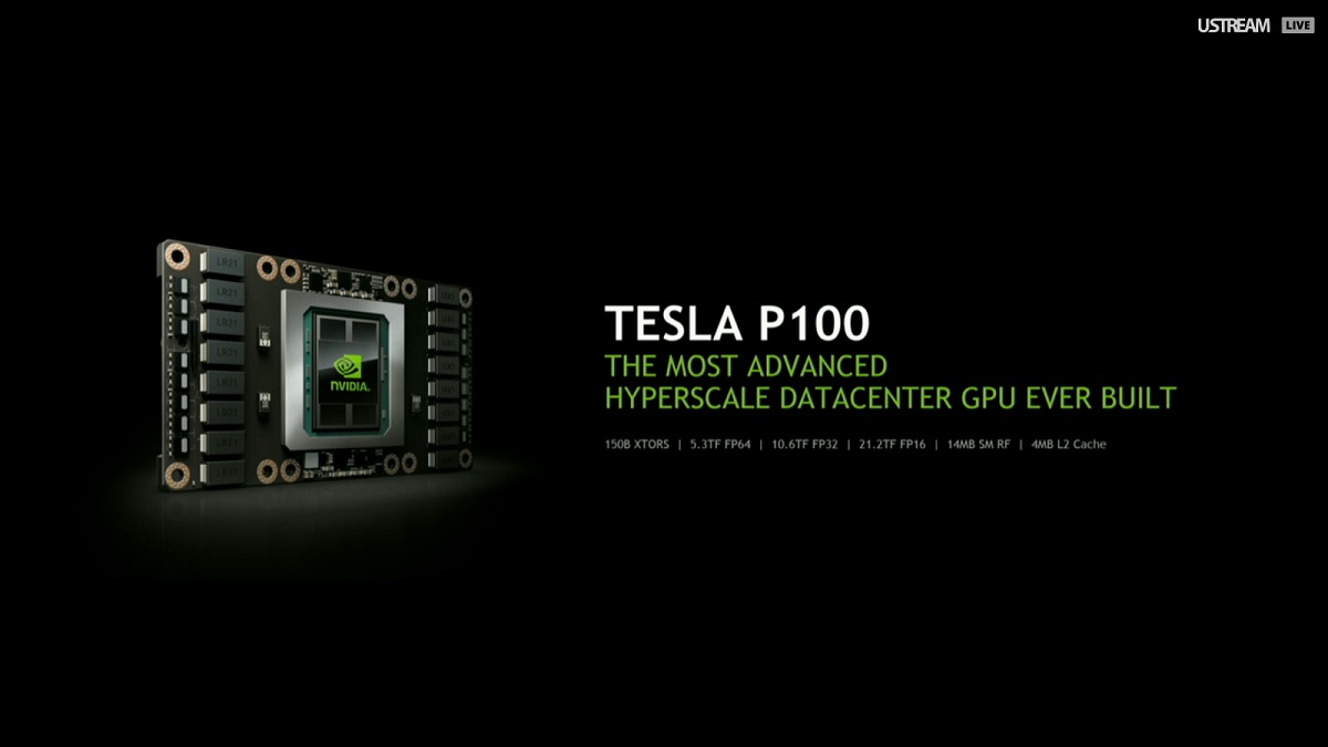
Nvidia has announced its most powerful GPU ever called the Tesla P100. The announcement was made during the company’s GPU Technology Conference which was held recently. Nvidia describes the Tesla P100 GPU as the most advanced hyperscale data centre GPU it has ever made. Despite not being made for average consumers, the Tesla P100 GPU does – roughly – show the capabilities of the Pascal microarchitecture.
Nvidia’s Tesla P100 is the first GPU in the world to feature the HBM2 memory standard by Samsung. In addition to that, the GPU also comes with a whopping 150 billion transistors, which are packed on a 610mm² die based on TSMC’s 16nm FinFet process. In comparison, the older GM200 Maxwell GPU only comes with 8 billion transistors.

According to Nvidia, its Tesla P100 GPU will come with 5.3 TFLOPS of FP64 performance (double-precision floating point); 10.6 TFLOPS of FP32 performance (single-precision floating point); and 21.3 TFLOPS of FP16 performance (half-precision floating point). To put it into perspective, the “consumer-grade” GeForce GTX Titan X comes with FP64 and FP32 performance of merely 0.2 and 7 TFLOPS. Then again, GPUs made for gaming do not need a large amount of precision point to begin with anyway.

Nvidia mentioned that mass production of the Tesla P100 GPU has begun and will be made available for OEMs by Q1 2017. Unfortunately, Nvidia hasn’t stated the price of its newest product; but from an average consumer point of view, it’s best to not know.
(Source: Fudzilla, TweakTown, Overclock3D)
Follow us on Instagram, Facebook, Twitter or Telegram for more updates and breaking news.


