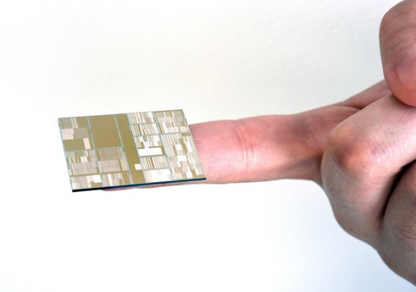
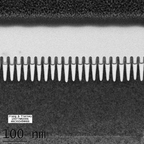
IBM has announced that it has managed to build new microprocessors based on a 7nm manufacturing process, the first major tech giant to breach the sub-10nm architecture.
2015 saw the introduction of chips made from the 14nm process, which can be found in Intel’s Core M processors as well as Samsung’s Exynos 7420 system-on-chip. These current-generation chips feature node transistors that are just 14 nanometers in size. This means that a 14nm chip holds more transistors that are more closely spaced together, lowering their capacitance and increasing overall efficiency compared to a 22nm chip of the same size.
IBM’s new 7nm chip further improves on the 14nm fabrication process. The working samples produced transistors that are 7nm in size – that’s 0.000000001m thick. As a comparison, a DNA string has a diameter of 2.5nm – almost three times smaller, but the significance here is the fact that these transistors are man-made. What’s more significant is the fact that the tech behemoth has broken the 10nm process barrier many are finding issues to overcome, by using a silicon-germanium (SiGe) channel material instead of pure silicon.
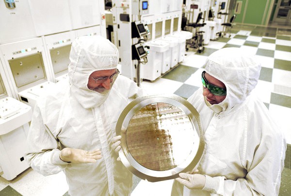
This is the first major breakthrough since IBM announced a $3 billion investment in R&D to develop a sub-10nm chip. Of course, the fact that these working samples have been made does not mean we’ll be seeing them powering the next big thing anytime soon. IBM says that they’re nowhere near ready for mass production, and are developed in research labs, not in the production line.
The Big Blue appears to have stolen a march from the likes of Intel and TSMC, where both have stated plans to develop commercially viable 10nm chips as early as 2016. As it stands, Intel’s Cannonlake 10nm chips have been put on hold due to difficulties working with chips that small, while TSMC has only mentioned that its 10nm chips will be ready in 2016. However, realistically speaking, we’ll probably only be seeing 7nm chips enter mass production closer to 2017 or 2018, as the industry continues the relentless pursuit of smaller and more efficient chips, whether by using SiGe materials or extreme ultraviolet (EUV) litography.
(Source: The Register, Ars Technica, The New York Times)


